Laygo setup for new technologies
This section describes how to setup laygo for a new technology. This document is written to help users create setup files and template libraries.
Example setup files
Instead of starting from scratch, you can reuse some parts of example files. Check the following repos for reference:
- cds_ff_mpt: https://github.com/ucb-art/BAG2_cds_ff_mpt
- NCSU freePDK45: https://github.com/ucb-art/BAG2_freePDK45
Overview
Following items are need to be set up laygo.
- BAG and PDK
- config files: laygo_config.yaml, layermap file (GDS only)
- template and grid library: (tech_name)_microtemplates_dense for most example generators, and associated yaml files
BAG setup
Since laygo exports the generated layout to BAG (unless you are exporting to GDS), you need to setup BAG before setting up laygo.
Note: Techinfo in BAG does not need to be set up because DummyTechinfo is used by default.
Config file (laygo_config.yaml)
Laygo uses laygo_config.yaml to store technology specific information. For each technology, user need to create/update laygo_config.yaml to contain correct parameters. An example laygo_config.yaml file for cds_ff_mpt technology is shown below.
#default_laygo_config file
metal_layers: #metal layers
- [M0, donotuse]
- [M1, drawing]
- [M2, drawing]
- [M3, drawing]
- [M4, drawing]
- [M5, drawing]
- [M6, drawing]
- [M7, drawing]
- [M8, drawing]
- [M9, drawing]
via_layers: #via layers
- [V0, donotuse]
- [V1, drawing]
- [V2, drawing]
- [V3, drawing]
- [V4, drawing]
- [V5, drawing]
- [V6, drawing]
- [V7, drawing]
- [V8, drawing]
pin_layers: #pin layers
- [text, drawing]
- [M1, pin]
- [M2, pin]
- [M3, pin]
- [M4, pin]
- [M5, pin]
- [M6, pin]
- [M7, pin]
- [M8, pin]
- [M9, pin]
prboundary_layer: [prBoundary, boundary] #boundary layer
tech_lib: cds_ff_mpt
text_layer: [text, drawing]
physical_resolution: 0.001
All fields need to filled in proper format, and contains information explained below:
- metal_layers (list): list of [layername, layerpurpose] of metal layers to be used for routing, starting from the bottom layer to the top layer.
- via_layers (list): list of [layername, layerpurpose] of via layers to be used for routing, starting from the bottom layer to the top layer.
- pin_layers (list): list of [layername, layerpurpose] of pin layers to be used for routing, starting from the bottom layer to the top layer.
- prboundary_layer (list): list of [layername, layerpurpose] of the prBoundary layer for placement.
- tech_lib (str): name of technology.
- text_layers (list): list of [layername, layerpurpose] of the text layer for annotations.
- physical_resolution (float): minimum layout grid resolution in micron. Most advanced nodes have grid resolutions ranging from 0.01 to 0.001.
(tech_lib).layermap (GDS flow only)
For GDS flow, a separate layermap file is needed to map the layer names to actual layer ids. Usually the layermap file is provided by Foundry and can be found in the PDK library (because the file is used to stream out a layout to a GDS file). Users can also try to make a layermap file by themselves. Here’s a example of the layermap file (numbers are not from any real/generic PDKs). For BAG flow this file is not needed.
#technology layer information for gds export
#you may find this in the cadence techlib directory
#layername layerpurpose stream# datatype
text        drawing 100 0
prBoundary  drawing 101 0
M1          drawing 1   0
M1          pin     1   1
M2          drawing 2   0
M2          pin     2   1
M3          drawing 3   0
M3          pin     3   1
M4          drawing 4   0
M4          pin     4   1
M5          drawing 5   0
M5          pin     5   1
M6          drawing 6   0
M6          pin     6   1
M7          drawing 7   0
M7          pin     7   1
M8          drawing 8   0
M8          pin     8   1
M9          drawing 9   0
M9          pin     9   1
VIA1        drawing 11   0
VIA2        drawing 12   0
VIA3        drawing 13   0
VIA4        drawing 14   0
VIA5        drawing 15   0
VIA6        drawing 16   0
VIA7        drawing 17   0
VIA8        drawing 18   0
Template library
Refer to Woorham’s Template library setup guide for more detailed instructions.
This is the most critical part of the laygo setup. Laygo uses hand-drawn templates of primitive devices and automatic generations are done in block levels. Therefore, users need to build the primitive templates and grids associated with the templates in advance. Template and grid cells in laygo are classified into 4 categories.
- Placement grids: defines the grid resolutions to place devices. prboundary_layer is used for specifying the resolution.
- Routing grids: defines the grid resolutions that routing wires and vias will be placed on. Rect objects with metal_layers are used to define the width / spacing / coordinate of the routing grid. Vias are placed at cross-sections of route wires, and they are constructed as via template cells.
- Device template cells: templates of devices will be placed on one of the placement grids. prboundary_layer is used to specify boundaries of the template, and pin_layers are used to specify pin regions and pin names.
- Via template cells: templates of vias will be placed on one of the route grids.
The figure shown below contains all types of template and grid cells.
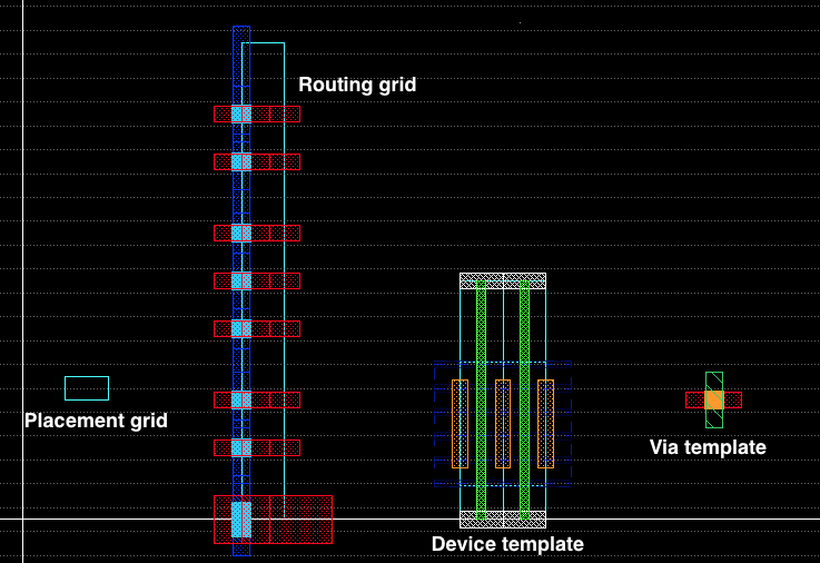 techex
Since there are no limitations on architecting grids, multiple placement grids / routing grids / devices / vias can be used for same technology / layer / device types. For example, 2 different types of grids (e.g thin and thick grids) can be used for Metal1-Metal2 grids. Or 2 different set of NMOS templates (short channel devices and long channel ones) can be constructed. These aspects are one of major differences from digital place and route flows.
The way of constructing template and grid cells is up to designer’s intent. However, there should be some levels of compatibility to enable code reusability over different technologies. We propose guidelines to architect template and grids cells for the reusability, especially for exampler scripts in the generators directory.
Template library name
For the generator examples, (tech_lib)microtemplates(flavor) is used for the primitive template library name. dense flavor is used for most example cases, which stands for optimized to reduce active area. For example, cds_ff_mpt_microtemplates_dense is the primitive template library name of cds_ff_mpt technology.
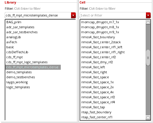 libname
Placement grids
placement_basic : a default placement grid layout. Contacted Poly Pitch(CPO) (for x axis) and a multiple of fin grid (for y* axis) are good candidates for the placement grid. Note that the size of any compatible templates should be a multiple of the placement grid.
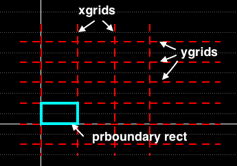 placement_basic
The figure above shows the placement_basic example for cds_ff_mpt technology. CPO was used for the x-resolution and fin grid was used for the y-resolution.
Routing grids and vias
route_M1_M2_basic : a default M1_M2_route grid cell. Minimum metal spacings and widths are used for the resolution and metal width, assuming vias can be placed in diagonal directions.
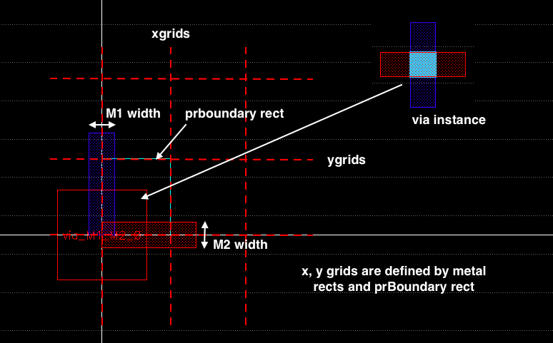 m1_m2_basic
route_M1_M2_basic_thick: an M1_M2 grid that is composed of thin M1 and thick M2. This grid is useful for power grid routings.
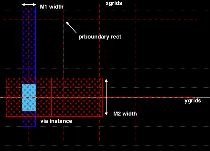 m1_m2_basic_thick
route_M1_M2_mos, route_M1_M2_cmos : M2_M2 grids that are designed to be compatible to NMOS/PMOS/CMOS stuctures. Note that grid coordinates are aligned to gate/drain/source pins of fets, and 2 horizontal tracks crosses the source and drain region.
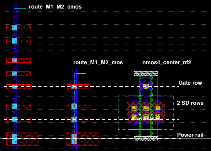 m1_m2_mos
M2_M3 grids (route_M2_M3_basic, route_M2_M3_thick_basic, route_M2_M3_cmos): M2_M3 grids that are compatible with M1_M2 grids.
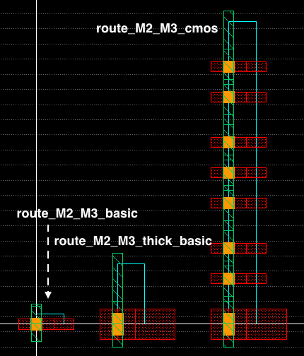 m2_m3
m2_m3Other grids on upper metal layers: following grids are used for example generators.
M3_M4 grids: route_M3_M4_basic, route_M3_M4_basic_thick, route_M3_M4_thick
M4_M5 grids: route_M4_M5_basic, route_M4_M5_thick
M5_M6 grids: route_M5_M6_basic, route_M5_M6_basic_thick, route_M5_M6_thick
Mosfet templates
Basic idea
In order to nicely capture all boundary design rules, all mostfet row structures are divided into 3 parts:
- Row boundary cells: placed at the (left & right) edges of device rows.
- Local boundary cells: placed between core devices
- Core cells: actual device cells (e.g. NF=2 NMOS, NF=1 NMOS, dummy NMOS, tap, …)
Any device row can be constructed by combining those element cells into one row.
 nmos
nmos
For generator examples, these types of cells need to be implemented: nmos4_fast, pmos4_fast, ntap_fast, ptap_fast
nmos4_fast family cells
Here are the list of nmos cells used in generator examples:
- nmos4_fast_left: left boundary of nmos4_fast row
- nmos4_fast_right: right boundary of nmos4_fast row
- nmos4_fast_boundary: local boundary of nmos4_fast primitives
- nmos4_fast_space, nmos4_fast_space: 1x spacing cells
- nmos4_fast_space_2x, nmos4_fast_space_nf2: 2x spacing cells
- nmos4_fast_space_4x, nmos4_fast_space_nf4: 4x spacing cells
- nmos4_fast_tap: nmos4 tap cell
- nmos4_fast_center_nf2: 2 finger nmos core
- nmos4_fast_center_nf2: 2-stacked nmos core
- nmos4_fast_center_nf2: 1 finger nmos core (gate left sided)
- nmos4_fast_center_nf2: 1 finger nmos core (gate right sided)
- nmos4_fast_center_nf2: 2 finger dummy nmos
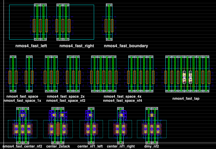 nmos_type
pmos4_fast family cells
Equivalent pmos cells need to be implemented as well:
- pmos4_fast_left: left boundary of pmos4_fast row
- pmos4_fast_right: right boundary of pmos4_fast row
- pmos4_fast_boundary: local boundary of pmos4_fast primitives
- pmos4_fast_space, pmos4_fast_space: 1x spacing cell
- pmos4_fast_space_2x, pmos4_fast_space_nf2: 2x spacing cells
- pmos4_fast_space_4x, pmos4_fast_space_nf4: 4x spacing cells
- pmos4_fast_tap: pmos4 tap cell
- pmos4_fast_center_nf2: 2 finger pmos core
- pmos4_fast_center_nf2: 2-stacked pmos core
- pmos4_fast_center_nf2: 1 finger pmos core (gate left sided)
- pmos4_fast_center_nf2: 1 finger pmos core (gate right sided)
- pmos4_fast_center_nf2: 2 finger dummy pmos
ptap_fast family cells
Ptap cells are used for constructing a ptap row, in order to construct thicker power grids (usually for pure analog cells) or guard rings.
- ptap_fast_left: left boundary of ptap_fast row
- ptap_fast_right: left boundary of ptap_fast row
- ptap_fast_boundary: local boundary of ptap_fast row
- ptap_fast_center_nf2: 2 finger ptap core
- ptap_fast_space: 1x spacing cell
- ptap_fast_space_nf2: 1x spacing cell
- ptap_fast_space_Nf4: 1x spacing cell
ntap_fast family cells
Equivalent ntap cells need to be implemented as well:
- ntap_fast_left: left boundary of ntap_fast row
- ntap_fast_right: left boundary of ntap_fast row
- ntap_fast_boundary: local boundary of ntap_fast row
- ntap_fast_center_nf2: 2 finger ntap core
- ntap_fast_space: 1x spacing cell
- ntap_fast_space_nf2: 1x spacing cell
- ntap_fast_space_nf4: 1x spacing cell
MOMCAP family cells
- momcap_boundary_1x: 1x momcap boundary
- momcap_center_1x: 1x momcap core
- momcap_dmy_1x: 1x momcap dummy (place where center cells are not placed)
- momcap_dmyblk_1x: 1x momcap dummy metal fill block cell
- momcap_dmyptn_mX_1x: 1x momcap dummy metal fill (mX) cell
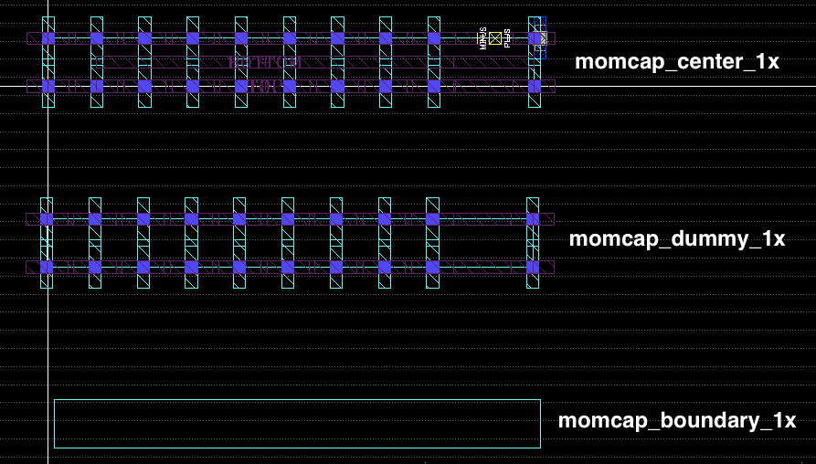 mom_type
Converting template layout to laygo database
After building all primitive templates, open bag and type
run laygo/labs/lab2_a_gridlayoutgenerator_constructtemplate.py
It will read the primitive template layouts and construct template / grid databases and save them to the following 2 yaml files:
* (tech_lib)_microtemplates_dense_templates.yaml
* (tech_lib)_microtemplates_dense_grids.yaml